Silicon photonics: On-chip waveguide and Si-Ge photodector [SP]
● Research fields
Photonic crystal & Metamaterials,
Meta-grating,
Ultrafast and Nonlinear optics,
Valley photonics.
● Research details
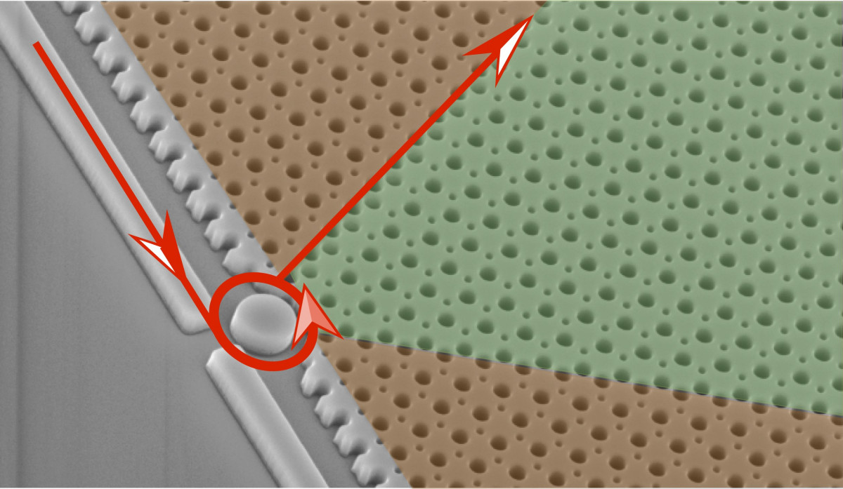
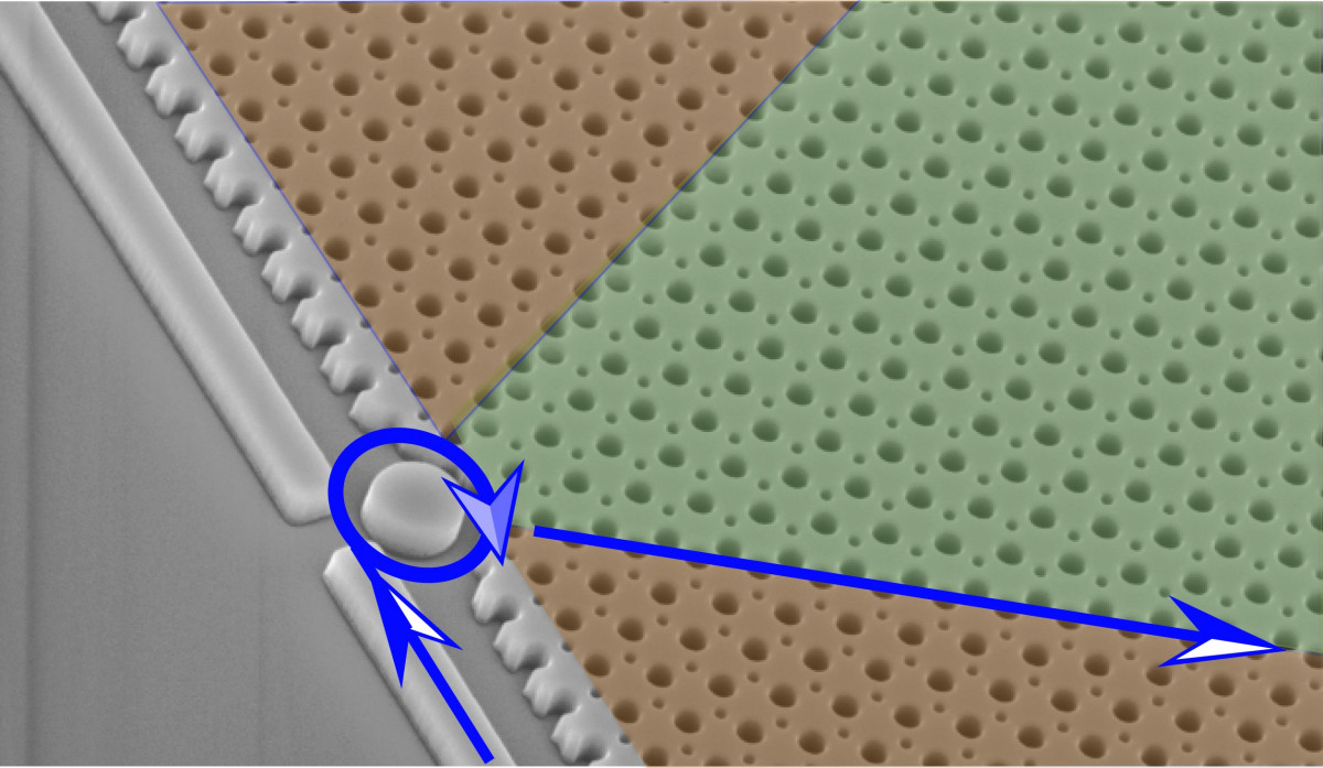
Silicon photonics shows outstanding ability to process light information on a single chip. Recent advances of topological physics provide a new paradigm to develop integrated nanodevices with robust light propagation and unidirectional coupling. This research is to promote the topological photonic crystal and meta-grating into the design of integrated devices, such as silicon-based waveguides and on-chip photodetector (PD). This project is supported by the National Key Research and Development Program of China. The candidates may have additional opportunity for a joint training PhD program with Europe (if you are good enough).
Sub-research 1: Design of on-chip waveguides and photodetector (PD) [SP1]
Engaging in (1) light information processing by using topological nanophotonic waveguides and (2) the design of Ge-Si photodetector based on topological optical effects. Besides of topological physics, the candidates will explore (1) the principle of optical communication in integrated photonics and (2) the basic principle of PDs, the simulations of photovoltaic effects in on-chip PDs. One may have the possibility for learning the nanofabrication techniques of semiconductor materials (e.g. Si, SiN, InP, Ge-Si).


Photonic routing based on topological waveguides
[1] Valley photonic crystals for control of spin and topology, Nat. Mat. 16, 298 (2017).
[2] A topological quantum optics interface, Science 359, 666 (2018).
[3] Terahertz topological photonics for on-chip communication, arXiv:1904.04213.
[4] Integrated lithium niobate electro-optic modulators operating at CMOS-compatible voltages, Nature 562, 101 (2018).
Sub-research 2: Measuring of silicon-based waveguides [SP2]
Engaging in the transient responses and nonlinear effects in topological integrated photonics. Besides of topological physics, the candidates will explore the optical experiments of streak camera, the nanofabrication techniques of semiconductor materials (e.g. Si, SiN, Ge), as well as light-matter interaction between 2D materials and topological nanophotonic structures.

An ultrashort pulse propagating along sharp-bending topological waveguides without distortion
[1] A silicon-on-insulator slab for topological valley transport, Nat. Commun. 10, 872 (2019).
[2] Ultrafast optical pulse shaping using dielectric metasurfaces, Science 364, 890 (2019).
[3] Direct Observation of Corner States in Second-Order Topological Photonic Crystal Slabs, Phys. Rev. Lett. 122, 233902 (2019).
● Required background
SP1: Electromagnetism, Semiconductor physics and device, Optical communications, Advanced Optics,
SP2: Basic/experienced skill in optical experiments. Interested in nonlinear optics and ultra-optics.
● Research suitability
PhD, MPhil, Undergraduate [Position SP1 and SP2]
● Contact supervisor
SP1: Professor Jian-Wen Dong (博导) dongjwen.at.SYSU, Doctor Xin-Tao He hext9.at.SYSU
SP2: Professor Fu-Li Zhao (博导) stszfl.at.SYSU, Doctor Xin-Tao He hext9.at.SYSU
